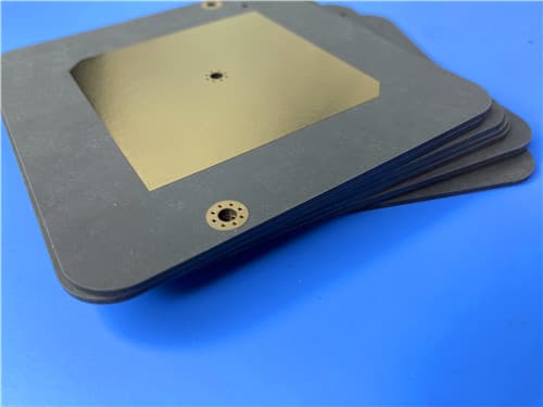
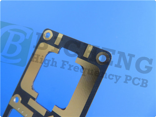
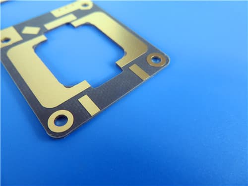
Rogers RT/duroid 5870 2-Layer 0.3mm ENIG PCB – Microstrip & Radar Applications
1. Introduction to RT/duroid 5870 PCB
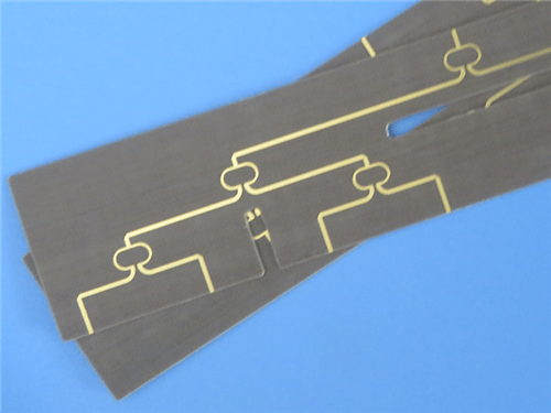
Rogers RT/duroid 5870 high frequency laminates are PTFE composites reinforced with glass microfibers, designed for exacting stripline and microstrip circuit applications. The randomly oriented microfibers result in exceptional dielectric constant uniformity.
The dielectric constant of RT/duroid 5870 laminates is uniform from panel to panel and is constant over a wide frequency range. Its low dissipation factor extends the usefulness of RT/duroid 5870 laminates to Ku-band and above.
RT/duroid 5870 laminates are easily cut, sheared and machined to shape. They are resistant to all solvents and reagents, hot or cold, normally used in etching printed circuits or in plating edges and holes.
This 2-layer rigid PCB is constructed entirely with RT/duroid 5870 as the core material, providing exceptional signal integrity, dielectric constant uniformity, and low-loss performance for demanding RF, microwave, and millimeter wave applications.
2. Key Features of RT/duroid 5870
Dielectric constant of 2.33 with tight tolerance ±0.02 at 10 GHz Dissipation factor of 0.0012 at 10GHz Temperature coefficient of dielectric constant (TCDk) of -115 ppm/°C Low Moisture Absorption of 0.02% CTE in X-axis of 22 ppm/°C, Y-axis of 28 ppm/°C and Z-axis of 173 ppm/°C Isotropic
3.Benefits of RT/duroid 5870 PCB
Uniform electrical properties over wide frequency range Easily cut, sheared and machined to shape Resistant to solvents and reagents used in etching or plating edges and holes Ideal for high moisture environments Well-established material Lowest electrical loss for reinforced PTFE material
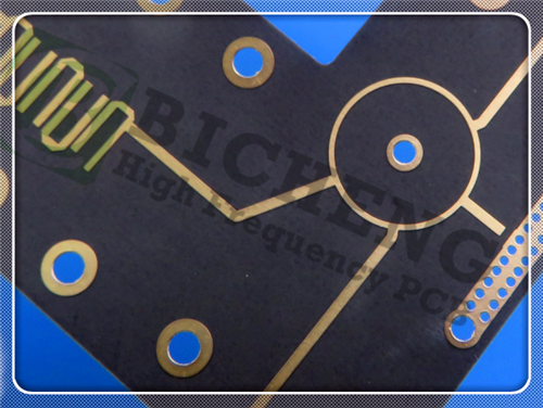
4.RT/duroid 5870 PCB Construction Details
| Item | Specification |
|---|
| Base material | RT/duroid 5870 |
| Layer count | 2 layers |
| Board dimensions | 85mm x 36mm = 1PCS, +/- 0.15mm |
| Minimum Trace/Space | 5/6 mils |
| Minimum Hole Size | 0.4mm |
| Blind vias | No |
| Finished board thickness | 0.3mm |
| Finished Cu weight | 1 oz (1.4 mils) outer layers |
| Via plating thickness | 20 μm |
| Surface finish | Electroless Nickel Immersion Gold (ENIG) |
| Top Silkscreen | No |
| Bottom Silkscreen | No |
| Top Solder Mask | No |
| Bottom Solder Mask | No |
| 100% Electrical test | Used prior to shipment |
5.PCB Stackup (2-Layer Rigid Structure)
Copper_layer_1 – 35 μm
RT/duroid 5870 – 0.254 mm (10 mil)
Copper_layer_2 – 35 μm
6.PCB Statistics
Components: 36
Total Pads: 56
Thru Hole Pads: 32
Top SMT Pads: 24
Bottom SMT Pads: 0
Vias: 28
Nets: 2
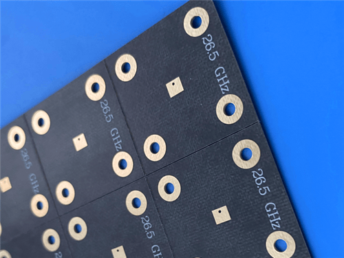
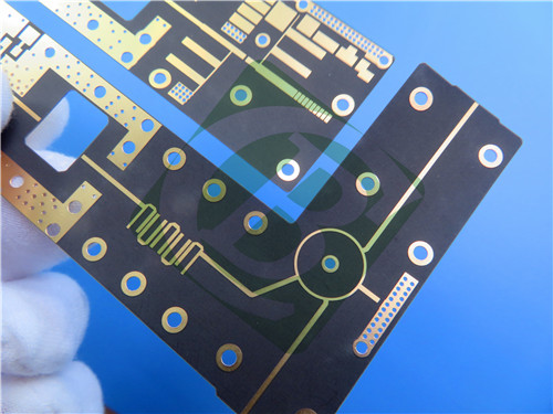
7.Primary Application Areas
Commercial Airline Broadband Antennas Microstrip and Stripline Circuits Millimeter Wave Applications Radar Systems Guidance Systems Point to Point Digital Radio Antennas
8.Quality Assurance
Artwork supplied: Gerber RS-274-X
Accepted standard: IPC-Class-2
Availability: Worldwide
 RTduroid 5870.jpg)
9.RT/duroid 5870 High Frequency Laminates – Product Introduction
RT/duroid® 5870 glass microfiber reinforced PTFE composites are designed for exacting stripline and microstrip circuit applications.
The randomly oriented microfibers result in exceptional dielectric constant uniformity.
The dielectric constant of RT/duroid 5870 laminates is uniform from panel to panel and is constant over a wide frequency range.
Its low dissipation factor extends the usefulness of RT/duroid 5870 laminates to Ku-band and above.
RT/duroid 5870 laminates are easily cut, sheared and machined to shape. They are resistant to all solvents and reagents, hot or cold, normally used in etching printed circuits or in plating edges and holes.
Normally supplied as a laminate with electrodeposited copper of ½ to 2 ounces/ft² (8 to 70μm) or reverse treated EDC on both sides, RT/duroid 5870 composites can also be clad with rolled copper foil for more critical electrical applications. Cladding with aluminum, copper or brass plate may also be specified.
When ordering RT/duroid 5870 laminates, it is important to specify dielectric thickness, tolerance, rolled, electrodeposited or reverse treated copper foil, and weight of copper foil required.
10.Features and Benefits
Key Features
Dielectric constant of 2.33 with tight tolerance ±0.02 at 10 GHz Dissipation factor of 0.0012 at 10GHz Temperature coefficient of dielectric constant (TCDk) of -115 ppm/°C Low Moisture Absorption of 0.02% CTE in X-axis of 22 ppm/°C, Y-axis of 28 ppm/°C and Z-axis of 173 ppm/°C Isotropic Td of 500°C TGA Thermal Conductivity of 0.22 W/m/K UL 94 V-0 flammability rating Lead-free process compatible
Benefits
Uniform electrical properties over wide frequency range Easily cut, sheared and machined to shape Resistant to solvents and reagents used in etching or plating edges and holes Ideal for high moisture environments Well-established material Lowest electrical loss for reinforced PTFE material
11.RT/duroid 5870 Data Sheet
| Property | Typical Value | Direction | Units | Conditions | Test Method |
|---|
| Dielectric Constant, εr (Process) | 2.33 ± 0.02 | Z | – | 10 GHz / 23°C | IPC-TM-650 2.5.5.5 |
| Dielectric Constant, εr (Design) | 2.33 | Z | – | 8 GHz – 40 GHz | Differential Phase Length Method |
| Dissipation Factor, tan δ | 0.0012 | Z | – | 10 GHz | IPC-TM-650 2.5.5.5 |
| Thermal Coefficient of εr | -115 | Z | ppm/°C | -50 to 150°C | IPC-TM-650 2.5.5.5 |
| Volume Resistivity | 2 × 10⁷ | Z | Mohm·cm | C96/35/90 | ASTM D257 |
| Surface Resistivity | 2 × 10⁷ | Z | Mohm | C96/35/90 | ASTM D257 |
| Specific Heat | 0.96 (0.23) | – | J/g/K (cal/g/°C) | – | Calculated |
| Moisture Absorption | 0.02 | – | % | 0.062" (1.6mm), D48/50 | ASTM D570 |
| Thermal Conductivity | 0.22 | Z | W/m/K | 80°C | ASTM C518 |
| Coefficient of Thermal Expansion (0-100°C) | 22 | X | ppm/°C | – | IPC-TM-650, 2.4.41 |
| Coefficient of Thermal Expansion (0-100°C) | 28 | Y | ppm/°C | – | IPC-TM-650, 2.4.41 |
| Coefficient of Thermal Expansion (0-100°C) | 173 | Z | ppm/°C | – | IPC-TM-650, 2.4.41 |
| Td | 500 | – | °C TGA | – | ASTM D3850 |
| Density | 2.2 | – | g/cm³ | – | ASTM D792 |
| Copper Peel Strength | 27.2 (4.8) | – | pli (N/mm) | 1 oz (35μm) EDC foil after solder float | IPC-TM-650 2.4.8 |
| Flammability | V-0 | – | Class | – | UL94 |
| Lead-Free Process Compatible | Yes | – | – | – | – |
12.Some Typical Applications
Commercial Airline Broadband Antennas Microstrip and Stripline Circuits Millimeter Wave Applications Radar Systems Guidance Systems Point to Point Digital Radio Antennas
13.Standard Thicknesses, Panel Sizes & Claddings
Standard Thicknesses
| Thickness (inch) | Thickness (mm) | Tolerance |
|---|
| 0.005" | 0.127 mm | ±0.0005" |
| 0.010" | 0.252 mm | ±0.0007" |
| 0.020" | 0.508 mm | ±0.0015" |
| 0.031" | 0.787 mm | ±0.0020" |
| 0.062" | 1.575 mm | ±0.0030" |
Standard Panel Sizes
18" × 12" (457 mm × 305 mm) 18" × 24" (457 mm × 610 mm) Additional panel sizes available
Standard Claddings (Electrodeposited Copper Foil)
Electrodeposited Copper Foil:
½ oz. (18 µm) HH/HH 1 oz. (35 µm) H1/H1
Rolled Copper Foil:
½ oz. (18 µm) 5R/5R 1 oz. (35 µm) 1R/1R
Additional claddings such as heavy metal, resistive foil and unclad are available
|
.jpg)
.jpg)